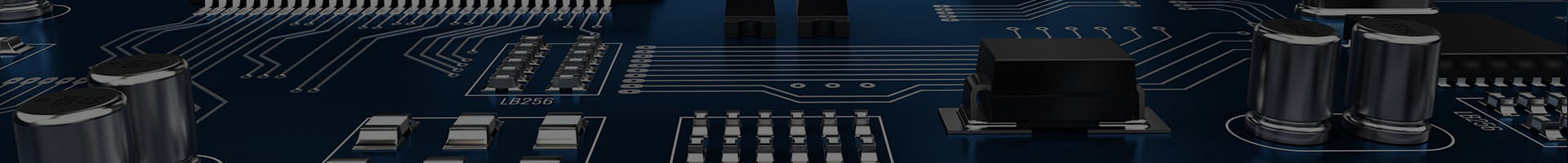
HDI PCB
What are HDI PCBs?
High Density Interconnect (HDI) printed circuit boards (PCBs) are defined as PCBs with higher wiring density per unit area than conventional PCBs. Nowadays, HDI PCBs are increasingly being used, and have made a big difference to technological advancement in electronics industry.
What are the benefits of HDI PCB?
HDI PCBs have many benefits for users over traditionally manufactured circuit boards. There are some benefits:
1. Excellent Versatility: High density interconnect circuit boards are typically used in applications in which weight, space, reliability, and performance are major concerns. Thus, HDI circuit boards are used in a wide range of applications that are related to aeronautics, consumer products, electronics, and computers.
2. Compact Designs: With HDI boards, you can secure more components on both sides of the raw PCB, allowing you to get more functionality out of a smaller space and expanding the overall capabilities of the equipment. HDI technology enables you to add functionality while reducing the size and weight of your products.
3. Improved Reliability: The smaller aspects ratios and the high-quality construction of microvias can increase the reliability of your board and your product. The improved performance and reliability HDI PCBs provide will lead to reduced costs and more satisfied customers.
4. Higher Signal Transmission: A shorter distance between components and a higher number of transistors can mean improved electrical performance. These features allow for lower power consumption, which improves signal integrity. Smaller sizes correlate to quicker signal transmissions and more significant reductions in overall signal losses and crossing delays.
5. Increased Cost-Effectiveness: With proper planning and manufacturing, HDI boards can be more cost-effective than other options because they require fewer raw materials due to their smaller size and the low number of layers they need. You’re able to get more functionality and value out of a smaller area and less material.
What are HDI PCBs Used?
The benefits explained above make these PCBs suitable for use in a number of applications, which include Medical Equipment, Industrial Control, Aerospace, consumer products and Military.
To know more about HDI PCBs, please contact us via Sales@flcircuits.com
PCB Capability
|
Item |
Mass Production |
Sample |
|
Max. Layers |
16layers |
30layers |
|
Max. Board Size |
21"x24" |
21"x26” |
|
Products Type |
2-layer PCB, multilayer PCB, Aluminum PCB, HDI PCB, Impedance PCB, HDI board PCB,BGA PCB, etc. |
2-layer PCB, multilayer PCB, Aluminum PCB, HDI PCB, Impedance PCB, HDI board PCB,BGA PCB, etc. |
|
Material |
FR4,CEM1,High Tg, Al base material, Copper base, etc. |
Rogers, Nelco, etc. |
|
Max. Board Thickness |
0.4mm~6.0mm |
<0.4mm and >7.00mm |
|
Min. Core Thickness |
0.10mm |
0.10mm |
|
Min. Track Width/Space |
4mil/4mil |
3mil/3mil |
|
Max. Copper Thickness |
Inner Layer: 6Oz |
Inner Layer: 8Oz |
|
Outer Layer: 8Oz |
Outer Layer: 10 Oz |
|
|
Min. Drill Size |
0.2mm |
0.15mm |
|
Min. Laser Drill Size |
0.1mm |
0.076mm |
|
PTH Diameter Tolerance |
±3mil |
±2mil |
|
Aspect Ratio |
8:1 |
12:1 |
|
PTH Wall Thickness |
18um-25um |
16um-35um |
|
Min solder mask bridge |
0.13mm |
0.10mm |
|
Min solder mask window |
0.10mm |
0.08mm |
|
V-cutting Tolerance |
±0.13mm |
±0.10mm |
|
Outline Dimension |
±0.13mm |
±0.10mm |
|
Warp and Twist |
≤0.7% |
≤0.5% |
|
Blinded and Buried Via Holes |
Yes |
Yes |
|
Controlled Impedance |
±10% |
±7% |
|
HDI Board |
1+N+1 |
2+N+2 |
|
Surface Treatment |
HASL |
HASL |
|
Surface Treatment |
HASL Lead Free |
HASL Lead Free |
|
Immersion Gold |
Immersion Gold |
|
|
Immersion Tin |
Immersion Tin |
|
|
Immersion Silver |
Immersion Silver |
|
|
Flash Gold |
Flash Gold |
|
|
OSP |
OSP |
|
|
Gold Finger |
Gold Finger |
|
|
Selective |
Selective |
PCB MANUFACTURING
Contact Us

Tel: +86-0755-23084786
E-mail: sales@flcircuits.com
Skype: +86-18902438891
Add: Building 7th, Gangtou Industry District, Shajing Town, Baoan Dist.Shenzhen, China


 Skype Chat
 Mail inquiry